Tag Archives: MOSFET

Tiny Tapeout 8

Tiny Tapeout is an educational project that makes it easier and cheaper than ever to get your designs manufactured on a real chip! Instead of paying 10,000 dollars for taping out a chip, enthusiasts and hobbyists can submit designs and share the floorplans in the same chips, dramatically reducing the per-design cost for individuals.

The final chip product shipped to me will include a chip on a carrier board and a demo board to communicate with the chip.

Since I have completed ChipCraft‘s 8-bit calculator course (Slide 157 Lab ID: C-EQUALS), I decided to submit this design to the Tiny Tapeout 8th iteration (TT8), which is due on September 6, 2024.

Because my design is coded with TL-Verilog, I followed Steve Hoover‘s tt08-makerchip-template and the 5-minute YouTube tutorial, which are extremely helpful.

My submitted TT8 design can be found at ezchips/tt08-my-calc (github.com) repository.

During the process of compiling my design, I did run into GDS Build issue with the following error:

/home/runner/work/tt08-my-proj/tt08-my-proj/src/project.sv:124: ERROR: Identifier `\L1_Digit[0].L2_Leds[0].L2_viz_lit_a0' is implicitly declared and `default_nettype is set to none.

Steve provided me with a neat trick by adding `default_nettype wire to the first \SV region of the project.tlv file, and it worked beautifully.

Here is the snapshot of a successful submission reported by TT08’s discord group:

It is really cool to have a 2D and 3D view of my design’s floor plan in the chip, which includes many semiconductor components like gates, flip-flops, multiplexers, etc.

Confused with 2’s Complement

While studying Udemy course “Digital Electronics & Logic Design Circuits” about 2’s complement and 1’s complement, I got puzzled with why all binary 1 (ex. 1111) is -1 in 2’complement, why positive 0 and negative 0 is same in 2’s complement, and why the range is different for 2’s and 1’s complements. I also had a misunderstanding that a negative number is the positive number with the most significant bit changed to 1, for example, -1 would be 1001.

Later, I learned the purpose of the complement system is mainly to perform subtraction through addition, for instance 7 – 2 is the same as 7 + (-2). It becomes straightforward by first listing positive numbers, and then listing individual negative numbers for 1’s and 2’s complements. I drew the following table with N=4 as an example and everything became clear.

It answers my questions:

  • Why 1111 is -1 in 2’s complement
  • Why 2’s complement solves the double zero issue
  • Why 1’s complement and 2’s complement have different ranges

Ohm’s Law Of Electrical Circuits Helped Me Understand CMOS

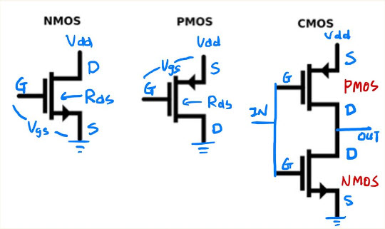
I often get confused with how NMOS or PMOS transistors output the logic “0” and “1”. One misconception I had is that I thought when NMOS or PMOS is in an “off” state, there should be an output. However, I missed an important fact that for a gate to transmit a clear output, the circuit must be able to conduct between Drain and Source. And it is in this sense that the resistance between D and S, the Rds, and the Ohm’s Law of electrical circuits helps me understand the case.

For NMOS, when Vgs is positive (as an input of logic “1”), the circuit becomes conductive. As the Rds becomes very low and essentially pulls the output (Drain) to the voltage close to ground, it transmits a clear logic “0”. When Vgs is zero or negative (as an input of logic “0”), the circuit becomes non-conductive, resulting in a high resistant Rds. Therefore, the voltage on output (Drain) becomes undefined, depending on the rest of the circuit that D is connected with.

On the other hand, for PMOS, when Vgs is negative (as an input of logic “0”), the circuit becomes conductive. As the Rds becomes very low and essentially pulls the output (Drain) to the voltage close to Vdd, it transmits a clear logic “1”. When Vgs is zero or positive (as an input of logic “1”), the circuit becomes non-conductive, resulting in a high resistant Rds. This causes the voltage on output (Drain) to become undefined, which, similar to NMOS, depends on the rest of the circuit that D is connected with.

By combining both PMOS and NMOS together as a CMOS, a clear output (Drain) of “0” or “1” can be transmitted with accordance to the signal from the input (Gate). This can be clearly shown in the NOT gate in the picture below.