
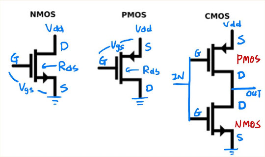
I often get confused with how NMOS or PMOS transistors output the logic “0” and “1”. One misconception I had is that I thought when NMOS or PMOS is in an “off” state, there should be an output. However, I missed an important fact that for a gate to transmit a clear output, the circuit must be able to conduct between Drain and Source. And it is in this sense that the resistance between D and S, the Rds, and the Ohm’s Law of electrical circuits helps me understand the case.
For NMOS, when Vgs is positive (as an input of logic “1”), the circuit becomes conductive. As the Rds becomes very low and essentially pulls the output (Drain) to the voltage close to ground, it transmits a clear logic “0”. When Vgs is zero or negative (as an input of logic “0”), the circuit becomes non-conductive, resulting in a high resistant Rds. Therefore, the voltage on output (Drain) becomes undefined, depending on the rest of the circuit that D is connected with.
On the other hand, for PMOS, when Vgs is negative (as an input of logic “0”), the circuit becomes conductive. As the Rds becomes very low and essentially pulls the output (Drain) to the voltage close to Vdd, it transmits a clear logic “1”. When Vgs is zero or positive (as an input of logic “1”), the circuit becomes non-conductive, resulting in a high resistant Rds. This causes the voltage on output (Drain) to become undefined, which, similar to NMOS, depends on the rest of the circuit that D is connected with.
By combining both PMOS and NMOS together as a CMOS, a clear output (Drain) of “0” or “1” can be transmitted with accordance to the signal from the input (Gate). This can be clearly shown in the NOT gate in the picture below.
Great insight! I would also recommend checking out “Circuit Intuitions: Looking into a Node” at https://www.eecg.utoronto.ca/~ali/intuitions.html.